![]()
|
|
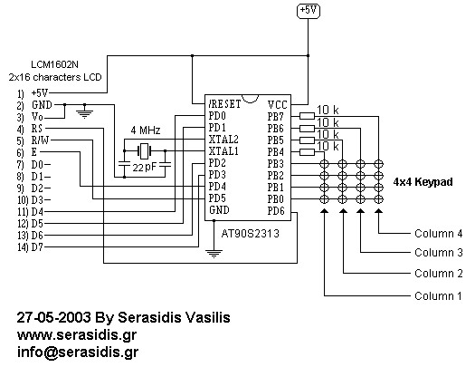
Scematic diagram of the circuit
Introduction
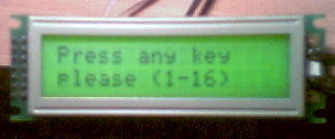
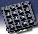
A very simple circuit for experiments with AT90S2313, 2x16 LCD display and 4x4 keypad. The clock is based on 4 MHz crystal, but you can use any other crystal between 1-4 MHz. The keys with the name "A", "B" ... "F" are typed to the LCD with numbers 10-16.
Because the AVR has only 15 I/O pins we work the LCD display with 4-bit data bus. The 4 resistors (10 k) are protecting the AVR from any shortcut on the columns of the keypad when AVR is scanning the keys by changing the pin status from input to output.
I wrote the source code in a simple form, that it means I haven't made any economy to the flash memory, for understanding the way how this circuit works.
How this is works
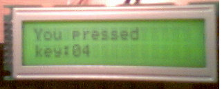
The AVR configure the PortB as PB0-PB3 inputs and PB4-PB7 outputs. On the beginning, the AVR puts the pin PB4 at logic '0' to enable the column 1 (the first 4 keys) and reads the status of the keys. If we have pressed any of the 4 first keys then the AVR sends the number of the key to the LCD display. If we have not pressed any of 4 first keys, the AVR puts the PB4 at logic '1' and PB5 at logic '0' to enable the second column. Reading the status of the keys and display the result to LCD, etc, until the 16th key is been read. After that, the circuit starts again to read from the 1st key (1st column) .
Download the schematic, hex and source code lcd_keys.zip