![]()
|
|
|
|
|
|
Features |
||
|
|
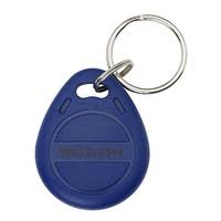
Picture 1: 125kHz RFID tag (key fobs) |
Picture 2: 125kHz RFID tag (credit card size). |

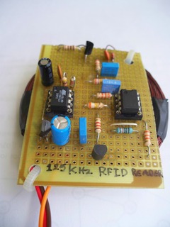
Introduction
This RFID reader works with 125 kHz tags in credit card size shape cards and with 125 kHz key fobs (picture 1). The EM4100 protocol is used. When you approach an RFID Tag close enough (4-5 cm) to the reader's coil (L1) the reader will read the 10-digit unique ID of the Tag and transmit it as ASCII characters trough the serial output with 2400 bits per second.
The circuit includes a buzzer that beeps when a Tag is read successfully.
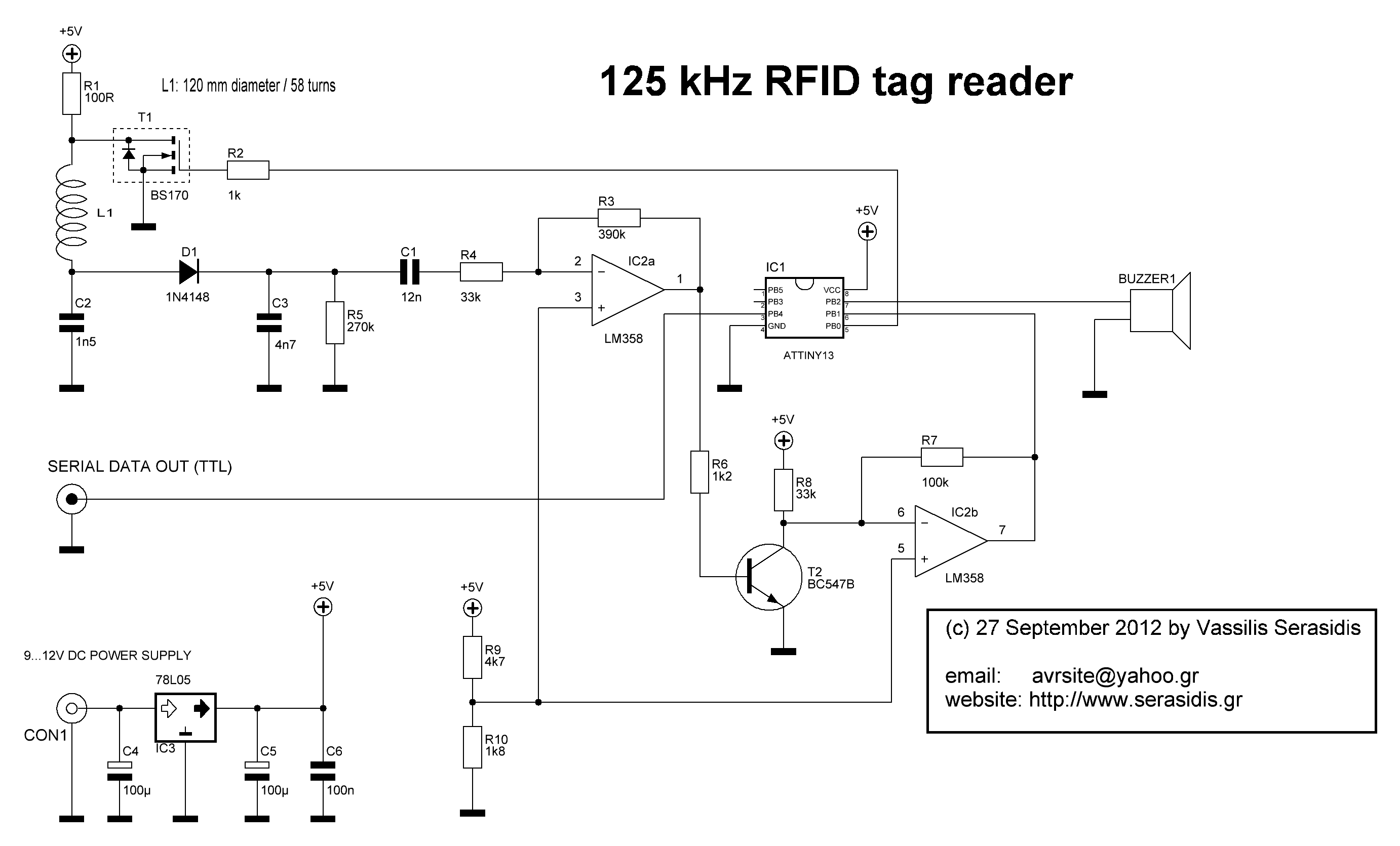
Schematic of the circuit (click to enlarge).
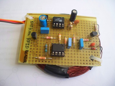
Description
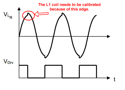
I will try to explain with simple words how the RFID works. The ATtiny13 uses the PWM function to produce an 125 kHz square wave signal. This signal comes out from PB0 pin. On the falling edge of the PB0 (Logic '0'), the T1 does not conduct. So the L1 is energized from R1 (100 ohm) with +5V. When PB0 pin rises (Logic '1') the T1 conducts and one side of L1 goes to GND. The L1 goes in parallel with C2 creating an LC oscillator. These transitions of L1 to logic '1' and logic '0' are made 125000 times in one second (125 kHz).
|
|
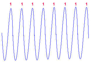
Picture 3: The 125 kHz waveform that is transmitted from L1 and C2 components.
The RFID reader provides energy to the transponder (Tag) by creating an electromagnetic field. The energy transmission between the RFID reader and the Tag is the same as transformers convert the voltage from the 220V AC power network to 12V AC, based on the magnetic field that creates the primary coil. In our case the primary coil is the RFID reader and the secondary coil is the RFID tag. The only difference is that on RFID circuits there is no iron core between the two coils (one coil is on the reader side and the other coil is in to the RFID tag). The D1 ,C3 and R5 components constitute an AM signal demodulator (AM = Amplitude Modulation) .
Data communication between Tag and reader.
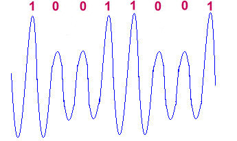
How an RFID Tag communicates with the reader? The idea is simple, but very clever! When a Tag wants to send a logic '0' to the reader it puts a "load" to its power supply line to request more power from the reader. That will make a small voltage drop on the RFID reader side. That voltage level is logic '0' (picture 4). Simultaneously, as long as the reader transmits the 125 kHz signal it reads the voltage of the transmitted signal trough the filters D1, C3 and R5, C1. When the Tag drops the voltage as we said before, the reader reads this voltage drop as logic '0'. When the Tag doesn't require any additional power, it doesn't make a voltage drop. That is logic '1' (picture 3). The 'Ones' or 'Zeros' length depends on the serial transmission data rate. For example, for 125 kHz carrier frequency we don't have 125000 bits per second data transmission! The data transmission from Tag to the reader varies from 500 bits per second up to 8000 bits per second.
|
Picture 4: Snapshot of transmitted data ...10101... |
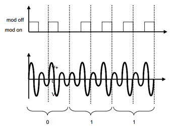
Picture 5: An alternative picture of the PSK modulation. |
The RFID tag content.
|
|
|
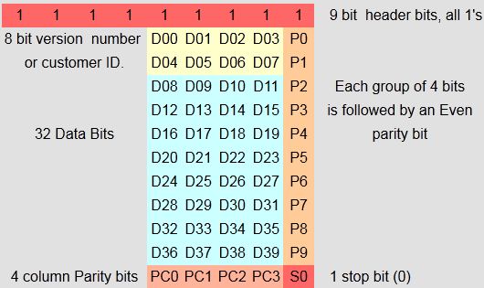
The data verification is been done from ATtiny13 by calculating the Even parity bit of each line and each column with the parity bits that had been received form the RFID Tag transmitted data.
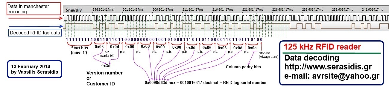
Example of RFID tag decoding. This example uses the RFID tag with serial number 0010016317
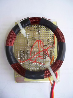
Constructing the coil
|
|
|
Programming the ATtiny13.
You have to set the ATtiny13 fuses to: High Fuse: 0x1F and Low Fuse: 0x7A .These settings set the ATtiny13 to work with the internal 9.6 MHz oscillator. The System clock divided by 8 option is disabled.
The firmware v1.00 is 1024 bytes and it occupies the 100% of the Flash program memory of ATtiny13.
Maybe a migration to any other 8-pin AVR such as ATtiny85 it would be a good idea if you want to add more functions to the source code.
Migration from ATtiny13 (1 kB flash memory) to ATtiny85 (8 kB flash memory) has been made on 13 February 2014 with firmware v2.00
Programming the ATtiny85.
You have to set the ATtiny85 fuses to: High Fuse: 0xDD and Low Fuse: 0xE2 .These settings set the ATtiny85 to work with the internal 8 MHz oscillator. The System clock divided by 8 option is disabled.
History:
|
(v2.01) 12 June 2014
|
* Oscillator frequency selection has been made automatic. The only you have to do is to select the micro-controller type from AVR studio 6 (ATtiny13 or ATtiny13A or ATtiny85) and re-compile the source code. * The baud rate has been changed from 2400 bps to 9600 bps. Of course you can change it back to 2400 bps if you want. |
|
(v2.00) 13 February 2014 |
The source code has been written from the scratch. The hex file is produced for ATtiny85 that has bigger flash memory and the same pinout with ATtiny13. |
|
(v1.00) 18 August 2012 |
The initial firmware version of 125 kHz RFID reader. |
|
|
v2.01 You can download the source code, hex file, schematic and pictures of 125 kHz RFID reader from here. |
-
Reference:
Created and published by Vassilis Serasidis on 21 May 2013